A group of researchers at ETH Zurich has developed a new technology that could represent an important step towards overcoming the limitations of bidirectional Fourier pixels. Pixels are the fundamental elements of every digital image, but not all perform the same function. Those that make up the screens of smartphones, computers and televisions serve to generate the images we see, while those present in camera sensors do the opposite, that is, they capture the light coming from the environment and transform it into digital information, exploiting the interaction between light and matter, a physical phenomenon also linked to the photoelectric effect. For decades these two functions have remained separate, so much so that displays and cameras are designed as separate components.
The result of their research is the Fourier pixel, a particular type of pixel capable of both displaying images and analyzing incoming light. In other words, the same element can simultaneously perform the role of display and optical sensor, a feature that could open up new perspectives in the field of applied optics.
The research is not about a new screen ready to hit the market or a camera destined to be integrated into next-generation devices. Instead, it is an experimental demonstration that shows how it is possible to design a pixel with much broader capabilities than those of traditional components. With further development, the Fourier pixel could find applications in areas ranging from next-generation displays and imaging systems to augmented reality devices and optical communications.
How the new Fourier pixel from ETH Zurich works
The operation of the Fourier pixel is based on light interference, a physical phenomenon that occurs when two or more light waves overlap. The same mechanism is also the basis of technologies such as holograms. Depending on how they combine, the waves can strengthen or partially cancel out, giving rise to well-defined light patterns. It is a phenomenon studied for over a century in optics and today used in various advanced technologies.
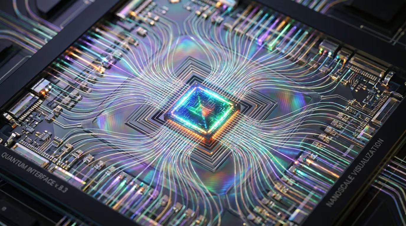
To exploit this, the researchers created tiny structures with dimensions in the order of nanometers on the surface of the device. When a beam of light passes through them, these structures transform part of the incident radiation into surface waves that propagate along the material. Subsequently, these waves are reconverted and, interfering with each other, generate light patterns that can be controlled with extreme precision.
What makes this new type of optical element different
The name Fourier pixel comes from Fourier analysis, a mathematical tool used to describe the behavior of waves. Thanks to this approach it is possible to design the geometry of the nanostructures so that the pixel produces a certain optical response. The same architecture, however, is not limited to controlling the output signal, but is also able to obtain information from what arrives from the outside.
In practice, the device not only detects the presence of light, but also analyzes some of its physical properties. This means that the same element can both produce a certain optical effect and interpret the received signal, a feature absent in conventional pixels. According to the authors of the study, it can in fact manage parameters such as phase and polarization, information that is particularly useful in numerous scientific and technological applications.
It is precisely this dual ability that distinguishes the Fourier pixel from traditional components: while those of a display simply emit or modulate light and those of a photographic sensor deal exclusively with detecting it, the new device integrates both functions in the same element.
What applications could this technology have?
Integrating multiple optical functions in the same component opens up interesting scenarios, even if they are yet to be explored. According to the researchers, the Fourier pixel could contribute to the development of more compact optical devices, reducing the number of elements needed to carry out operations that today require separate systems.
Hypothesized applications include intelligent displays, capable not only of showing images, but also of collecting data on the surrounding environment, and new imaging systems capable of analyzing the characteristics of light with greater precision. This architecture could also prove useful in augmented reality and mixed reality devices, where available space is limited and integrating multiple functions into the same element represents an important advantage.
Another possible area of use concerns optical communications. Since the Fourier pixel is designed to manipulate and detect the properties of light, it could in the future also be used in systems that transmit information through light signals. However, these are developments that will require further studies before they can be transformed into concrete applications.
Because this technology will not arrive on smartphones and monitors immediately
Although the result obtained by the researchers is promising, the Fourier pixel is still a prototype developed in the laboratory. The study highlights the feasibility of the concept, but it does not mean that this solution is ready to be used in consumer products.
One of the main obstacles concerns the complexity of its implementation. The tiny structures that allow the pixel to control and analyze light must be manufactured with extremely precise nanofabrication techniques, very different from those used to produce common displays for smartphones and monitors.
Even the conditions in which the prototype was tested are far from those of an electronic device used in everyday life. The experiments were conducted in a controlled environment and with an optical setup specifically designed to demonstrate how the technology works. Before it can be transformed into a commercial component it will therefore be necessary to overcome numerous engineering challenges, from miniaturization of the system to large-scale production.
For the moment, therefore, the Fourier pixel represents above all a demonstration of the potential offered by optical engineering. Further research will be needed to understand whether this solution can be adopted in everyday devices, but the result obtained to date demonstrates that the very concept of pixels can evolve, paving the way for more versatile optical devices capable of performing functions that were previously considered separate.